- 您现在的位置:买卖IC网 > Sheet目录2006 > LTC2451ITS8#TRPBF (Linear Technology)IC ADC 16BIT DELTA SIG TSOT23-8
LTC2451
12
2451fg
Discarding a Conversion Result and Initiating a New
Conversion with Optional Configuration Updating
At the conclusion of a conversion cycle, a write cycle
can be initiated. Once the write cycle is acknowledged, a
STOP (P) command initiates a new conversion. If a new
configuration is required, this data can be written into the
device and a STOP command initiates a new conversion
(see Figure 8).
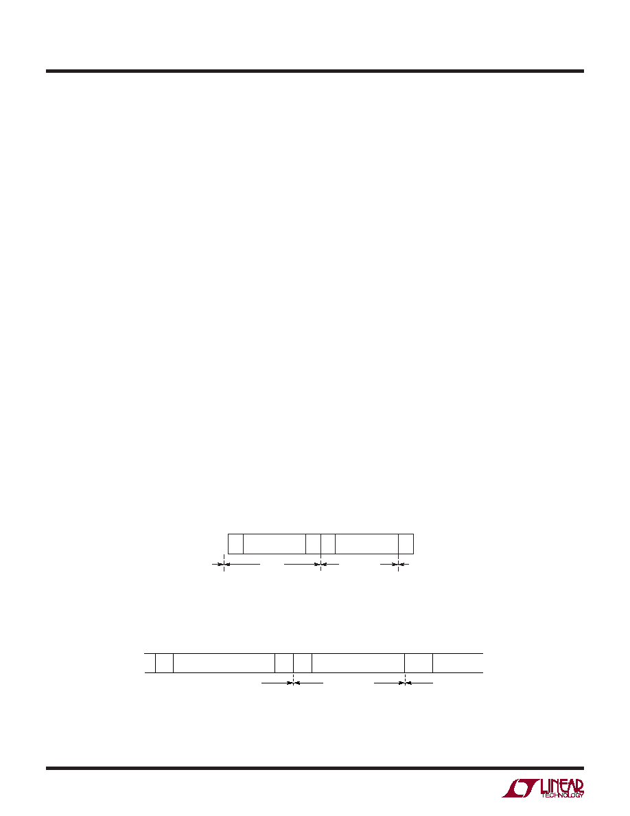
Synchronizing the LTC2451 with the Global Address Call
The LTC2451 can also be synchronized with the global
address call (see Figure 9). To achieve this, the LTC2451
must first have completed the conversion cycle. The
master issues a START, followed by the LTC2451 global
address 1110111, and a write request. The LTC2451 will
be selected and acknowledge the request. If desired, the
master then sends the write byte to program the 30Hz
or 60Hz mode. After the optional write byte, the master
ends the write operation with a STOP. This will update
the configuration registers (if a write byte was sent) and
initiate a new conversion on the LTC2451, as shown in
Figure 9. In order to synchronize the start of the conver-
sion without affecting the configuration registers, the
write operation can be aborted with a STOP. This initiates
a new conversion on the LTC2451 without changing the
configuration registers.
PRESERVING THE CONVERTER ACCURACY
TheLTC2451isdesignedtodramaticallyreducetheconver-
sion result’s sensitivity to device decoupling, PCB layout,
antialiasing circuits, line and frequency perturbations.
Nevertheless, in order to preserve the high accuracy capa-
bility of this part, some simple precautions are desirable.
Digital Signal Levels
Due to the nature of CMOS logic, it is advisable to keep
input digital signals near GND or VCC. Voltages in the
range of 0.5V to VCC – 0.5V may result in additional cur-
rent leakage from the part.
Driving VCC and GND
In relation to the VCC and GND pins, the LTC2451 com-
bines internal high frequency decoupling with damping
elements, which reduce the ADC performance sensitivity
to PCB layout and external components. Nevertheless, the
very high accuracy of this converter is best preserved by
careful low and high frequency power supply decoupling.
A 0.1F, high quality, ceramic capacitor in parallel with a
10F ceramic capacitor should be connected between the
VCC and GND pins, as close as possible to the package.
The 0.1F capacitor should be placed closest to the ADC.
Figure 8. Start a New Conversion without Reading Old Conversion Result
APPLICATIONS INFORMATION
Figure 9. Synchronize the LTC2451 with the Global Address Call
SLEEP
7-BIT ADDRESS
(0010100)
WRITE
(OPTIONAL)
S
P
W ACK
DATA INPUT
CONVERSION
2451 F08
GLOBAL ADDRESS
(1110111)
SLEEP
CONVERSION
S
W
ACK
WRITE (OPTIONAL)
P
2451 F09
DATA INPUT
发布紧急采购,3分钟左右您将得到回复。
相关PDF资料
LTC2452ITS8#TRPBF
IC ADC 16BIT DELTA SIG TSOT23-8
LTC2453ITS8#TRMPBF
IC ADC 16BIT DELTA SIG TSOT23-8
LTC2482IDD#TRPBF
IC ADC 16BIT 10-DFN
LTC2483IDD#TRPBF
IC ADC 16BIT I2C 10-DFN
LTC2485CDD#TRPBF
IC ADC 24BIT I2C 10-DFN
LTC2487CDE#PBF
IC ADC 16BIT DELTA SIG 14-DFN
LTC2492IDE#TRPBF
IC ADC 24BIT DELTA SIG 14-DFN
LTC2493IDE#TRPBF
IC ADC 24BIT DELTA SIG 14-DFN
相关代理商/技术参数
LTC2452CDDB#PBF
制造商:Linear Technology 功能描述:ADC Single Delta-Sigma 60sps 16-bit Serial 8-Pin DFN EP 制造商:Linear Technology 功能描述:Bulk
LTC2452CDDB#TRMPBF
功能描述:IC ADC 16BIT DELTA SIG 8-DFN RoHS:是 类别:集成电路 (IC) >> 数据采集 - 模数转换器 系列:- 产品培训模块:Lead (SnPb) Finish for COTS
Obsolescence Mitigation Program 标准包装:1 系列:- 位数:10 采样率(每秒):357k 数据接口:DSP,MICROWIRE?,QSPI?,串行,SPI? 转换器数目:1 功率耗散(最大):830µW 电压电源:单电源 工作温度:-40°C ~ 85°C 安装类型:表面贴装 封装/外壳:10-WFDFN 裸露焊盘 供应商设备封装:10-TDFN-EP(3x3) 包装:剪切带 (CT) 输入数目和类型:2 个单端,单极;2 个单端,双极;1 个差分,单极;1 个差分,双极 产品目录页面:1396 (CN2011-ZH PDF) 其它名称:MAX1395ETB+TCT
LTC2452CDDB#TRPBF
功能描述:IC ADC 16BIT DELTA SIG 8-DFN RoHS:是 类别:集成电路 (IC) >> 数据采集 - 模数转换器 系列:- 标准包装:2,500 系列:- 位数:16 采样率(每秒):15 数据接口:MICROWIRE?,串行,SPI? 转换器数目:1 功率耗散(最大):480µW 电压电源:单电源 工作温度:-40°C ~ 85°C 安装类型:表面贴装 封装/外壳:38-WFQFN 裸露焊盘 供应商设备封装:38-QFN(5x7) 包装:带卷 (TR) 输入数目和类型:16 个单端,双极;8 个差分,双极 配用:DC1011A-C-ND - BOARD DELTA SIGMA ADC LTC2494
LTC2452CTS8#PBF
制造商:Linear Technology 功能描述:Bulk 制造商:Linear Technology 功能描述:MS-ADC/Delta Sigma, CUT TAPE 16-bit 60Hz SPI Different Ultra-Tiny Delta Sigma ADC
LTC2452CTS8#TRMPBF
功能描述:IC ADC 16BIT DELTA SIG TSOT23-8 RoHS:是 类别:集成电路 (IC) >> 数据采集 - 模数转换器 系列:- 标准包装:1 系列:microPOWER™ 位数:8 采样率(每秒):1M 数据接口:串行,SPI? 转换器数目:1 功率耗散(最大):- 电压电源:模拟和数字 工作温度:-40°C ~ 125°C 安装类型:表面贴装 封装/外壳:24-VFQFN 裸露焊盘 供应商设备封装:24-VQFN 裸露焊盘(4x4) 包装:Digi-Reel® 输入数目和类型:8 个单端,单极 产品目录页面:892 (CN2011-ZH PDF) 其它名称:296-25851-6
LTC2452CTS8#TRPBF
功能描述:IC ADC 16BIT DELTA SIG TSOT23-8 RoHS:是 类别:集成电路 (IC) >> 数据采集 - 模数转换器 系列:- 标准包装:2,500 系列:- 位数:16 采样率(每秒):15 数据接口:MICROWIRE?,串行,SPI? 转换器数目:1 功率耗散(最大):480µW 电压电源:单电源 工作温度:-40°C ~ 85°C 安装类型:表面贴装 封装/外壳:38-WFQFN 裸露焊盘 供应商设备封装:38-QFN(5x7) 包装:带卷 (TR) 输入数目和类型:16 个单端,双极;8 个差分,双极 配用:DC1011A-C-ND - BOARD DELTA SIGMA ADC LTC2494
LTC2452IDDB#PBF
制造商:Linear Technology 功能描述:ADC Single Delta-Sigma 60sps 16-bit Serial 8-Pin DFN EP 制造商:Linear Technology 功能描述:Bulk
LTC2452IDDB#TRMPBF
功能描述:IC ADC 16BIT DELTA SIG 8-DFN RoHS:是 类别:集成电路 (IC) >> 数据采集 - 模数转换器 系列:- 产品培训模块:Lead (SnPb) Finish for COTS
Obsolescence Mitigation Program 标准包装:1 系列:- 位数:10 采样率(每秒):357k 数据接口:DSP,MICROWIRE?,QSPI?,串行,SPI? 转换器数目:1 功率耗散(最大):830µW 电压电源:单电源 工作温度:-40°C ~ 85°C 安装类型:表面贴装 封装/外壳:10-WFDFN 裸露焊盘 供应商设备封装:10-TDFN-EP(3x3) 包装:剪切带 (CT) 输入数目和类型:2 个单端,单极;2 个单端,双极;1 个差分,单极;1 个差分,双极 产品目录页面:1396 (CN2011-ZH PDF) 其它名称:MAX1395ETB+TCT